
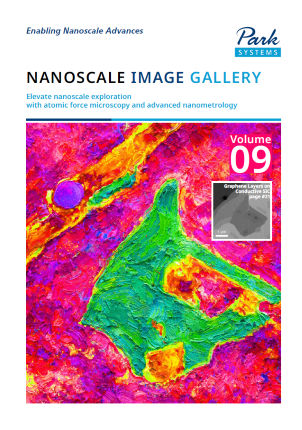
Image Gallery 2026, Vol.09
01. Atomic Force Microscopy Topography Imaging
- Suspended TMDC Monolayer
- Laminated Steel
- MoS2 Flake on TEM Grid
- AR/VR Optics Display Structure
- Display-Related Structures
- Defect on PR Patterns
- Mobile Display Panel
- Wafer Edge (Edge Bead Removal Region)
- 300 mm Wafer Edge
02. Atomic Force Microscopy Advanced Imaging Modes
- LFM: Perylene Tetracarboxylic Diimide
- PinPoint™: MoS2 Bubbles
- C-AFM: Epi Wafer
- C-AFM: Monolayer Graphene
- C-AFM: Logic Wafer
- C-AFM: SRAM
- KPFM, DFRT-PFM: 2-Layer hBN on Graphene
- KPFM: Self-Assembled Molecular Layer
- KPFM: Graphene Layers on Conductive SiC
- PFM: CuInP2S6
- MFM: GdFe Thin Film
- MFM: Square Spin Ice Lattice
- MFM: Metal Alloy
- TFM, LFM: Few Layer Graphene
- TFM: MoS2
- TFM: Twisted Trilayer Graphene
- TFM: Twisted Bilayer Graphene - 1, 2, 3
- PiFM: PS/PVAC Blend
- PiFM: Graphite and h-BN
- PiFM: Teflon Defect
- PiFM: Si/SiO2 Pattern
- FiM: Cu Pad Wafer
- PCM, KPFM, C-AFM: Perovskite
- SECCM: Glassy Carbon
- Nano Probing, KPFM, C-AFM: Few Layer Graphene
03. Imaging Spectroscopic Ellipsometry (ISE) Applications
- WS2 Flake on Si/SiO2 (300 nm) Substrate
- Cr/Au/Fe3GeTe2/Al Multilayer Structure
- β-Lacto Globuline on SiO2 Substrate
- CoFeB/MgO
04. Digital Holographic Microscopy Applications
- Self-Assembly of Micro Rafts
- MEMS Accelerometer and Gyroscope
- Cardiomyocyte
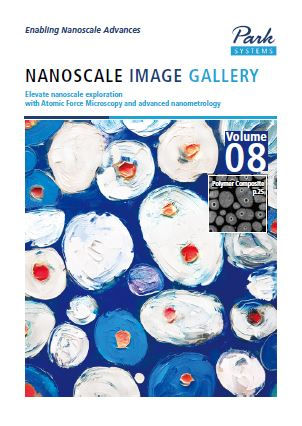
Image Gallery 2025, Vol.08
01. Atomic Force Microscopy Topography Imaging
- Display Backplane (LTPS TFT)
- RGB Cells Black Matrix
- Tandem Solar Cell
- FTO Glass
- Microlens Array
- GaN epi Defect on Sapphire Substrate
- Electrodeposited Copper Foil for Flexible PCB
- Nanodots on Si
- Chemical Etched Titanium Disc
- STO (110)
- InAs Quantum Dots embedded on a GaSb Substrate
- Post TiN Etch
- Cu Pad(Dishing Analysis, Type 1, Type 2)
- EUV Mask: Soft Defect Repair
- Semiconductor Failure Analysis
- Organic Molecules
- Hydrogel
- Polymer Composite
- Self-assembled Block Copolymer
- Hyper-branched Polymer
- Polystyrene Beads on Mica
- mRNA
- Purple Membrane of Bacteriorhodopsin
02. Atomic Force Microscopy Advanced Imaging Modes
- Perovskite
- WTe2 on Au Electrode
- Leakage Current of Ceramic Layer
- Poly Silicon
- Trapped Bubble in Twisted Bilayer Graphene on hBN
- MoS2 Atomic Lattice Structure
- Single Layer Graphene on hBN
- Moiré Pattern in Twisted Bilayer Graphene on hBN
- Moiré Superlattice in Twisted Bilayer Graphene on hBN
- P-N Dopant Sample with Different Concentration
- PMOS and NMOS Plug
- MOSFET
- Tailored Cutting and Isolation of Graphene Flake
- Solar Cell with Different Anti-Reflection Properties
- Ge ALE on Patterned Wafer
- Trench MOSFET
- Li-ion Battery on Si Substrate
- Moiré Patterns on Folded hBN
- Patterned Wafer
- Comparison of Hair before and after Treatment
- Polyethylene Terephthalate (PET)
- Organic Molecules
- PS-LDPE
- Floppy Disk
- Tissue
- 2205 Stainless Steel
- Artificial Spin Ice Lattices (B, H)
- Magnetic Material Patterned Wafer
- Pt/Co hBN
- Permalloy
- e-Beam Damage on ArF PR
- Defect
03. Imaging Spectroscopic Ellipsometry (ISE) Applications
- Trapped Bubble in Twisted Bilayer Graphene on hBN
- MoSe2-WSe2 Lateral Heterostructure
- Residuals on Si Wafer after Water Cleaning Process
- Anisotropic Organic Crystals
- Exfoliated Molybdenum (IV) Telluride
- Lanthanum Nickel Oxide Layers
- Printed ALD TiO2 Structures
- 20 nm Al2O3 Coated LHAR Chip
Image Gallery 2024, Vol.07
01. Atomic Force Microscopy Topography Imaging
- GaN-based LED
- Micro LED
- FinFET
- Epitaxial silicon fin
- Few layers MoS2 on SiO2/Si
- Melem molecules on HOPG
- Few layers of MnBi2Te4 (MBT)
- Tungsten disulfide (WS2)
- GaAs on PSS
- Ion beam etched MgO trench
- Molds for Nanoimprint; Hole structure
- Molds for Nanoimprint; Pillar structure
- PR trench patterns
- Mask repair
- Defects of LiNbO3 waferli>
- Poly Silicon (p-Si)
- Zirconia (ZrO2)
- Steel (1-2)
- AgCl/Al2O3 catalyst treated metal surface
- Dental implant screw
- Ceramic
- Nano Au on epithelial cells
- Plant protein amyloid fibril
- DNA origami (1-2)
- Adenovirus
- Adenovirus with DNA bundle
- Bacteriophage
- Mycelium growth on pattern
- PCB
- PCB treated by silver nanoparticles
- Poly (allylamine hydrochloride) (PAH)
- Membrane filters in liquid
- Polymer electrolyte membrane (PEM)
- Contact lens
- Crystal originated particle (COP) defect
- Epi stacking fault (ESF) defect
- Diced silicon wafer with etched trench
02. Atomic Force Microscopy Advanced Imaging Modes
- Tungsten disulfide (WS2)
- Twisted hBN bilayer
- CVD-grown MoS2
- Graphene on hBN (1-3)
- Twisted bilayer graphene on hBN (1-2)
- Multi-layer graphene (1-2)
- Graphene transferred wafer
- DRAM test sample with 68 nm channel
- Melamine cyanurate
- Lithium battery diaphragm (Separator)
- SrRuO3 (SRO) on SrTiO3 (STO) substrate
- LCD panel
- PMN-PT
- Ferrimagnetic Alloy (GdFe)
- Portrait of Jamsetji Tata lithography
- Wreath decoration lithography
03. Imaging Spectroscopic Ellipsometry (ISE) Applications
- Graphene grown by CVD
- MOSFET device
- Residual glass
- Methylammonium-Lead-Bromide-Perovskite
- 2D Subwavelength periodic structure
- USAF1951 resolution test sample
- Rewritable color nano-prints in Sb2S3 films
- Diamond defects
- Optical switch of Sb2S3
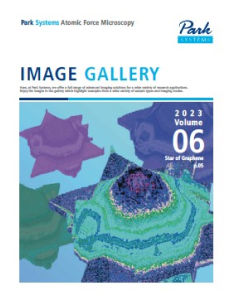
Image Gallery 2023, Vol.06
01.Topography
- Trapped water between
- Graphene & hydrophilic substrate
- Star of Graphene
- Defect of LiNbO3
- GaN epi wafer
- GaN on Si epi film
- Semi-fluorinated alkanes
- Nanostructures on polymer
- P(VDF-TrFE-CFE)
- Moire pattern of MoS2-WSe2
- Cowpea chlorotic mottle viruses (CCMV)
- Adenovirus
- Plate-shaped DNA origami
- Collagen fibrils
- Bacteria Klebsiella pneumoniae (KP)
- Escherichia coli (E. coli)
- Crosslinked starch & pectin fibers
- Sunflower pollen
- Diamond with plated / gold nickel
- CMP test key
- WLI image of wafer ID mark
- TSV Cu pad oxidation
- Chip
- Stitched image of Chiplet
- MoSi2 Hard defect repair
- Hard defect repair of photomask
- MoS2 film
- Suspended silicon nitride membrane
- Mo film
- AR Lens
- Copper film
- Fractals of silver nanoparticles
- Ceramic-Portland cement
02.Advanced mode
- Trapped water between
- Graphene & hydrophilic substrate
- Star of Graphene
- Defect of LiNbO3
- GaN epi wafer
- GaN on Si epi film
- Semi-fluorinated alkanes
- Nanostructures on polymer
- P(VDF-TrFE-CFE)
- Moire pattern of MoS2-WSe2
- Cowpea chlorotic mottle viruses (CCMV)
- Adenovirus
- Plate-shaped DNA origami
- Collagen fibrils
- Bacteria Klebsiella pneumoniae (KP)
- Escherichia coli (E. coli)
- Crosslinked starch & pectin fibers
- Sunflower pollen
- Diamond with plated / gold nickel
- CMP test key
- WLI image of wafer ID mark
- TSV Cu pad oxidation
- Chip
- Stitched image of Chiplet
- MoSi2 Hard defect repair
- Hard defect repair of photomask
- MoS2 film
- Suspended silicon nitride membrane
- Mo film
- AR Lens
- Copper film
- Fractals of silver nanoparticles
- Ceramic-Portland cement
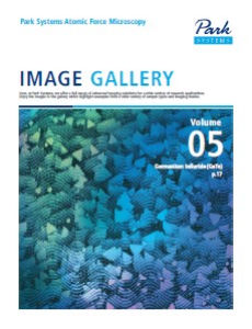
Image Gallery 2022, Vol.05
01.Topography
- C36H74 on HOPG
- Molecular network on HOPG
- Isotactic polypropylene
- Graphene/hBN heterostructure
- tBN+MLG
- Di-Phe-Phe nanotubes
- Block copolymer
- SBS
- PS-PVAc
- GeTe
- NiO on ITO glass
- Organosilane SAM
- BaTiO thin film
- Defects on Si wafer
- GaN LED wire
- Line/Space patterns
- Auto stitched WLI image
- SOI wafer
- Epitaxial gallium nitride (epi-GaN) film
- Dendrimer
- Blood cell
02.Advanced mode
- MLG-hBN , tBG+bBN
- LiNbO3
- All-solid-state Li ion battery
- PZT thin film
- Aluminium TX630 alloy
- CAM on HOPG
- F H14 20
- Boron nitride on monolayer graphene
- SRAM
- Ta/ NiFe /Ta microman
- PS-PMMA block copolymer
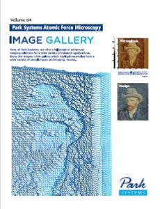
Image Gallery 2021, Vol.04
01.Topography
- Mica composite flake
- Vincent van Gogh by e-beam litho
- NbGaO3 with 0.4 nm terraces
- ADS510 on hBN/SiO2
- Polytetrafluoroethylene (PTFE)
- Water droplet on HOPG
- Moiré pattern of Graphene on hBN
- Exfoliated Graphene on SiO2
- Patterned surface of epitaxial SiC
- F14H20 on Si
- 3D NAND flash
- Post CMP wafer
- Semiconductor process monitoring; CMP
- Semiconductor process monitoring; Annealing
- Semiconductor process monitoring; Exposure
- Failure analysis; Defect analysis
- Failure analysis; Position uniformity
- Damage of PR patterns
- LiNbO3 wafer
- Copper foil
- GaN film
- ITO coated Quarts chip
- Si grating
- Fun grating
02.Advanced mode
- F14H20 on Si; Potential
- Dot lithography on PZT; Potential
- Park logo lithography on PZT; Potential
- F14H20 on Si; Work function
- BFO; PFM Images
- PMN-PT; PFM Images
- PMN-PT; Piezo response curves
- HfO2; Electrical property
- SAM on Au; STM
- Au patterned PET; STM
- Rubber with iron particles; Magnetic property
- LDPS/PE; Thermal property
- Vincent van Gogh; lithography
- Santa with Rudolph; lithography
- Christmas tree and firework; lithography
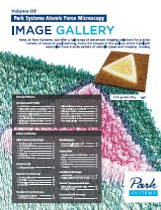
Image Gallery 2020, Vol.03
01.Standard Modes
- True Non-Contact⢠Mode
- Self-assembly of semi-fluorinated alkanes
- Nanopatterned graphene on boron nitride
- Suspended single-layer graphene
- MoS2 layers on SiO2
- Supramolecular polymer
- ITO film sputter deposited onto silicon
- Aligned fibers
- AIN/GaN/AIN hetero structure
- HfO2 into ITO (Indium Tin Oxide) film
- Al2O3-doped CaMnO3
- SnS2 Flakes
- Trench etch profile on MESA
- Trench etch profile on Si wafer
- Cannabidiol molecules
02.Advanced mode
- Kelvin Probe Force Microscopy
- MoS2 layers on SiO2
- CVD grown WS2
- HOPG
- F14H20 on Si
- PS/PVAc film
- ER 316L stainless steel
- Conductive AFM
- FAPbl3 perovskite film
- Megnetic Force Microscopy
- ER 316L stainless steel
- Fe thin films
- Ferromagnetic nanobars array
- Fe-Nd-B alloy
- Piezoelectric Force Microscopy
- Composite barium titanate
- PVDF fibrous membrane
- Nanolithography
- Taegeuk mark lithography on PZT
- Christmas ball lithography on Si
- Tapping Mode
- Monolayer graphene on PDMS surface
- MoS2
- F14H20
- C36H74
- PS/LDPE (Phase)
- Margarines
- Lateral Force Microscopy
- PS/LDPE (LFM)
- Single-crystal SrTiO3 (001) after annealing
- PinPoint™ Nanomechanical Mode
- Block copolymer embedded in rubber
- TPU plastic thin film
- Scanning Thermal Microscopy
- PS/LDPE (SThM)
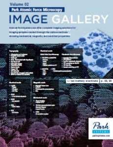
Image Gallery 2019, Vol.02
01.Topography
- Lithography on Si substrate
- Tungsten coated wafer
- Hydro gel
- Ecoli, Ecoli treated with Cirpofloaxin
- Red Blood Cell
- DNA, DNA Protein
- Polyaniline (PANI)
- Styrene beads
- Copper Foil
- BFO (BiFeO3)
- STO (SrTiO3), Annealed LAO(LaAlO3)
- BiVO4 on treated YSZ substrate
02.Advanced mode
- Al-Si-Au
- HOPG
- MoS2
- Polymer patterns on Si
- HfO2
- MoS2
- Hair
- Phthalocyanine praseodymium
- Annealed Phenanthrene
- BFO (BiFeO3)
- DLaTGS Pyroelectric detectors
- PZT nanotubes on Nb-STO
- PZT thin film
- Domain switching on PZT
- Floppy
- ITO glass
- CNT Film
- Li ion battery electrode
- SiC MOSFET
- HOPG Moire
- SiC Device
- Magnetic Vortex Core
- Co/Cr/Pt
- Phthalocyanine praseodymium
- NiFe
- Polymer on Si
- Blended Polymer
- Crystal Facetts
- Si nanowire on glass

Image Gallery 2018, Vol.01
01.Topography
- Plasmid DNA in liquid
- Polyvinylidene fluoride beads
- Polymers
- Microchannel pattern
- Calcium hydroxyapatite
- Polytetrafluroethylene membrane filter
- AEAPDES self-assembled monolayer
- Hexacontene
- Chromium-gold surface
- Graphene on boron nitride
- Lithium niobate wafer
- Topological insulator film
- Silicon carbide film
- Hard disk media
- Imprint Sample
- Bacteria
- Sperm with defect
- Adhesive systemr
02.Advanced mode
- Polydimethylsiloxane liquid crystal
- Block copolymer I
- Block copolymer thin film
- Block copolymer II
- Block copolymer III
- Polymer blend with nanofibers
- Block copolymer phase change by temp
- Kevlar fiber
- Graphene on Cu
- Lithography o n c ompact disk
- Metallo DNA system with silver(I) inserted
- Device failure analysis
- SRAM
- MoS2
- Multi-layer ceramic capacitor
- 100 nm lead zirconate titanate Film
- Polyvinylidene fluoride film
- BTO
- Lead magnesium niobate
- - lead titanate single crystal
- Magnetic patterned array
- Boron nitride thin film on silicon