开尔文探针力显微镜 (KPFM)
表面电势的高分辨率和高灵敏度成像
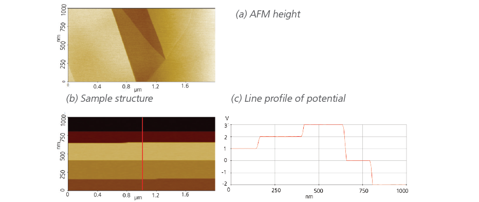
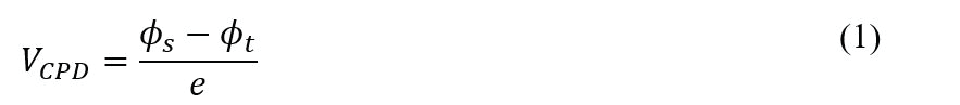
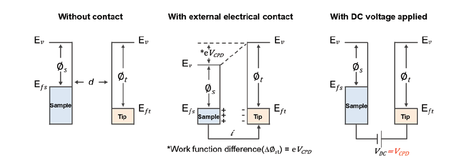
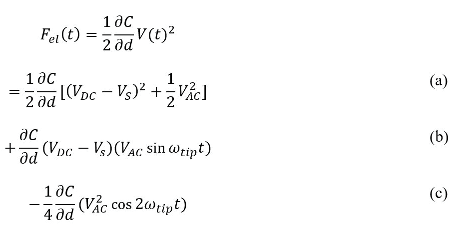
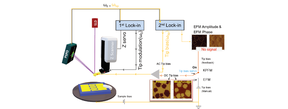
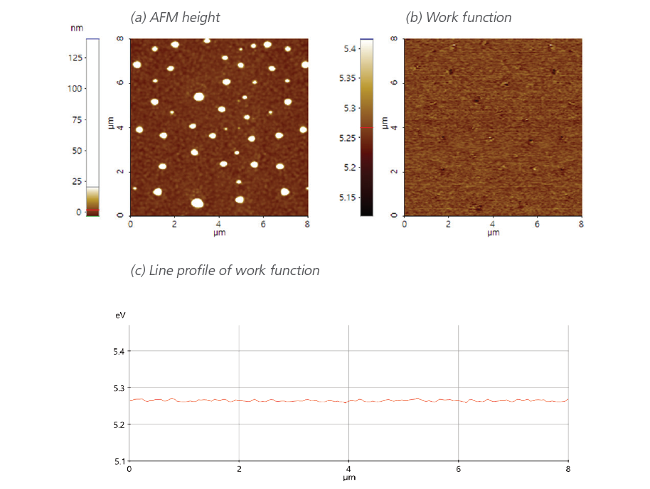
KPFM(开尔文探针力显微镜)的原理与带有DC偏压反馈的增强EFM(静电力显微镜)相似。DC偏压由反馈回路控制,以将ω项归零。将力归零所需的DC偏压是表面电势的测量值。区别在于从锁相放大器获得的信号的处理方式。 如前一节所述,从锁相放大器获得的ω信号可以用以下方程表示。这个ω信号本身可以用于测量表面电势。当VDC = Vs时,即DC偏压电压与样品的表面电势相匹配时,ω信号的幅度为零。可以在系统中添加反馈回路,并改变DC偏压电压,使得测量ω信号的锁相放大器的输出为零。这个将ω信号归零的DC偏压电压值就是表面电势的测量值。通过这个DC偏压电压的变化创建的图像代表表面电势的绝对值。
x